
If you’re involved in the engineering of products manufactured globally, chances are you’ve been personally affected by SNAFU’s on an epic scale. Despite your best efforts, you probably had to sacrifice some weekends, or late nights, or quality time with your kiddos, or at the very least, your blood pressure.
Hey, it happens to the best of us, especially if that global manufacturing involves China in any way . . . but before you give up on your blood pressure entirely, let me ask you this: have your best efforts involved TELEPORTATION?
Before we go over the modern magic of teleportation possible in R&D today, let’s get clear on the process that’s supposed to happen in an ideal world.
First, some socially inept nerds virtually dream up how a physical design should theoretically work in their engineering cave. (It’s OK, maybe you can’t say that, but I can. I used to be that guy.)

They might not ever touch a physical component in their design work! To the layman onlooker, it might all appear to be math and video games. That’s mostly because it is.
Usually, there are several disciplines involved in this theoretical design stage. The discipline that dictates the other requirements for the system often begins and then hands off specs to the other departments. In electro-optical systems, usually, the optical design is the thing you do first. Then the optical engineer (that was me) would tell the mechanical nerds about the size and location needed for the optics. Also, the optics guys often would tell the electrical engineers about how much juice they need running to an LED, or how much light will turn on a sensor. Then, after those informational batons were passed, the ME’s (mechanical engineers) and EE’s (electrical engineers) would go to work in their own engineering caves to design their respective pieces of the system. Those caves might be down the hall from each other, or they might be on different continents. I’ve lived both scenarios.
Once those circuit designs, mechanical designs, and optical designs are all finished, detailed prints (“blueprints”, but no one actually says that) are often handed over to a factory in some country where stuff is really cheap to manufacture. This might be Mexico, or China, or Thailand, or somewhere else that isn’t the place where the parts were engineered.
Then, everyone waits a while for those parts to be physically made on a different part of the globe and then shipped half-way around the world. Hopefully, it’s not MF Chinese New Year at the time. It usually is Chinese New Year, though. It just seems to work out that way. So, your 6-week lead time might turn into 8-10 weeks in that case.

After the parts arrive back where either the assembly happens or where one of the engineering disciplines live or both, all the pieces are put together physically for the first time! Fingers are crossed. Everyone hopes that when all the parts are connected up and the switch is flipped, the thing a.) does not catch fire, and b.) works like it was intended to.
Of course, everything all working together seamlessly on the first try and on time is a laughable fairytale of a dream.
Maybe the components you used had lousy, inaccurate info on the manufacturer’s spec sheet. Maybe the system ran hotter than your thermal simulations predicted (if you even ran those) and consequently, your LED’s aren’t as bright as they need to be. Maybe your mechanical drafter was working in the wrong units when he created some component and it’s totally in the wrong place in the system. Maybe China put the wrong color LED’s on the circuit board. (Come on, automobile turn signals are not green, China. THEY ARE NEVER GREEN.) Maybe China used the wrong material. Maybe China used the wrong resistors. Maybe China mislabeled a driver. Maybe . . . China.
And maybe . . . maybe on that slow boat from whatever country your components were manufactured in . . . maybe the things just fell off the boat. Like, literally fell off the boat and sank to the bottom of the ocean. That also seriously happens.
Here is a PowerPoint slide I created to illustrate the real-life global R&D process to a bunch of high school mechatronics students in Silicon Valley I lectured to recently. Pretty accurate, and I think they got it:

What happens then, after all those hiccups? Hopefully, the project managers involved had the foresight enough to factor in both multiple design iterations and random China screw-ups. Yet, sometimes, when all the things go wrong at once, even if your Gantt chart had some cushion in it, your project ends up months behind. Then what?!
Well, if your product is low-tech and not timing-critical, maybe you just push out that anticipated release date.
However, if your product is, say, a 2018 Cadillac Escalade, it needs to be ready to roll by 2018. Otherwise, if it comes out in 2019, it is not a 2018 Cadillac Escalade! So what then?
Well, then comes shouting, migraines, missed birthday parties of your children, high blood pressure, occasional heart attacks (no joke) and the tears of fully grown men (also not a joke). Seriously, I’ve seen more grown men cry than I’d like to recall. 98% of those instances were in professional engineering settings.

Or . . . or you can salvage some of that lost time with teleportation!
Teleportation?!
Yeah! Well, kind of. It’s more like the next best thing.
With the technology available today, we don’t have to wait on manufacturing in another part of the globe before we figure out if a design itself is valid! Your engineers in the USA and Europe and Timbuktoo can all (nearly) instantly have each other’s designs physically in-hand. Moments after a design iteration is figured out in Munich, the parts in that design can begin to be physically created in real reality in San Diego. Actually, those designs can be immediately made into tangible parts in more than one place. Today, you can teleport AND CLONE prototype parts, too!
How is this possible?! If you haven’t figured it out yet, I’m not really talking about teleportation (ORLY?) – – I’m talking about rapid prototyping of parts using 3D printers and PCB printers.
If several R&D facilities scattered across the globe have the same rapid prototyping equipment, they can shoot electronic blueprints of new part ideas to each other at the speed of light! Then, engineers can create and hold in their hands nearly identical copies of those parts and begin assembling and testing entire systems before China ever turns on injection molding or SMT machines.
3D printing along with the more general processes of additive manufacturing have been around for a while. It’s just now, though, that the quality of the parts possible and the variety of materials make so many of a design’s mechanical parts teleport-able. You can print metal parts! You can print optical quality lenses (https://www.luxexcel.com/)! You can print parts with carbon fiber or even Kevlar (http://impossible-objects.com)!
Printing circuit boards is a much newer thing to become easily accessible — especially if your design uses flex boards. If you’re not familiar, flex boards look like this, and they’re . . . well . . . flexible circuit boards:
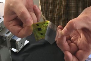
Other older technologies are available to mill out circuit boards from rigid substrates, but they’re messy and can’t make these fancy flex boards which for many applications can’t be substituted in the prototyping stage.
BotFactory takes a unique approach to this in that their desktop PCB prototyping machines print conductive and insulating inks to build multiple conductive layers (like the wires of a circuit board). All their machines come standard with pick-and-place capability, too, so that means you could create the totally completed circuit board – with all your components on it – that France dreamed up and turned into a Gerber file minutes ago, right now from your desk in the USA . . . Or, Timbuktoo. (Whatever, you do you! I’m typing this from Bermuda, so hey.)
When I came across BotFactory’s technology, I thought back to all those migraines and man tears when China completely messed up a circuit board. I thought about all those weekends I lost when I had to make up for wasted time in the prototyping stages of electro-optic system design. And then I thought,
“engineers need this! Me from yesterday needs this!”
So now, I’m helping to spread the word about BotFactory‘s amazing tech. If you want to be able to print out and assemble multi-layer PCB boards, even flex boards, from your desktop and save gobs of development time in the iterative prototyping phase of R&D, shoot me an email. I’d be happy to learn about your current challenges and talk with you how teleportation technology can help:
erin.mcdermott@botfactory.co
You can check out their site here: https://www.botfactory.co
Now, is this teleportation stuff a substitute for testing first production parts made in Asia? Unfortunately, no. You still have to make sure China didn’t swindle you on material quality and put the right parts on all the things, and etc, in the stuff they’ll ultimately make for you in mass production. But for the most time-consuming system design phases, especially within multi-national corporations, you could easily save months in a project. Literally months!
Plus, perhaps most importantly, for the optical enginerd near and dear to my heart, that’s less time proving a Chinese factory screw up was to blame for a system failure and not an optical design.
You’re welcome, don’t cry, and I love you.